Thin films – typically below 1 μm in thickness – are the foundation of modern electronics, optics and advanced surface engineering. Compared with bulk materials, thin films can be tuned for specific electrical, optical, magnetic and protective properties, which makes them essential for semiconductors, sensors, optical filters, energy devices and protective coatings.
Among many deposition methods, three technologies dominate high-value thin film fabrication today:
- PVD – Physical Vapor Deposition
- CVD – Chemical Vapor Deposition
- ALD – Atomic Layer Deposition
This article walks through how each process works, their key variations (electron-beam evaporation, magnetron sputtering, PECVD, PE-ALD), and the pros and cons that matter when you’re choosing between PVD vs CVD vs ALD for a real application.
各类沉积技术的层级关系-1024x813.webp)
- 1. Thin Film Deposition in a Nutshell
- 2. PVD vs CVD vs ALD at a Glance
- 3. Physical Vapor Deposition (PVD)
- 4. Chemical Vapor Deposition (CVD)
- 5. Atomic Layer Deposition (ALD)
- 6. Choosing Between PVD, CVD and ALD
- 7. From Thin Films to Real Components: Why This Matters
- 8. Conclusion
- Surface Treatment Services with Certified Quality and Environmental Management
- Aluminum Die Casting Services
1. Thin Film Deposition in a Nutshell
A thin film is a solid layer with thickness from a few nanometers to about 1 μm, deposited on a substrate. Because film properties depend strongly on:
- composition and microstructure
- thickness and uniformity
- interface with the substrate
deposition technology has a direct impact on device performance and reliability.
Modern thin films are used in:
- Magnetic information storage
- Microelectronics and integrated circuits
- Optical coatings and filters
- Catalysts and energy devices (e.g., fuel cells, solar cells)
- Display and sensor technologies
To engineer these films, we mainly rely on gas-phase deposition methods – PVD, CVD and ALD – which all use vapor-phase precursors but differ in how material is generated and how it grows on the surface.
2. PVD vs CVD vs ALD at a Glance
A useful way to compare PVD, CVD and ALD is to look at step coverage vs deposition rate:
- PVD offers high deposition rates but relatively poor step coverage in deep trenches or high-aspect-ratio structures.
- CVD gives medium deposition rates and better conformality, especially in optimized processes.
- ALD delivers near-perfect step coverage and thickness control, but at the cost of very slow deposition rates.
In other words:
- Need speed on relatively simple surfaces? → PVD.
- Need high-quality, dense films at reasonable throughput? → CVD / PECVD.
- Need atomic-level control in ultra-complex 3D structures? → ALD / PE-ALD.
The next sections go deeper into each method.
3. Physical Vapor Deposition (PVD)
3.1 Principle and Process Steps
Physical Vapor Deposition is performed in vacuum. A solid or liquid source material is physically transformed into a vapor (atoms, molecules or ions), transported through low-pressure gas, and then condensed on a substrate to form a thin film.
A generic PVD process has three core steps:
- Vapor generation – evaporation / sputtering
- Energy is applied to the source so that atoms are released into the gas phase.
- Transport
- The vapor travels through vacuum (sometimes assisted by plasma) toward the substrate.
- Deposition and film growth
- Atoms or ions condense and nucleate on the surface, then grow into a continuous film.
Two major industrial PVD families are evaporation (including electron-beam evaporation) and sputtering (often magnetron sputtering).
3.2 Electron-Beam (E-Beam) Evaporation
In electron-beam evaporation, a focused high-energy electron beam generated by an electron gun bombards the source material in a crucible. The intense localized heating causes the material to melt and then evaporate; the vapor travels to and condenses on the substrate.
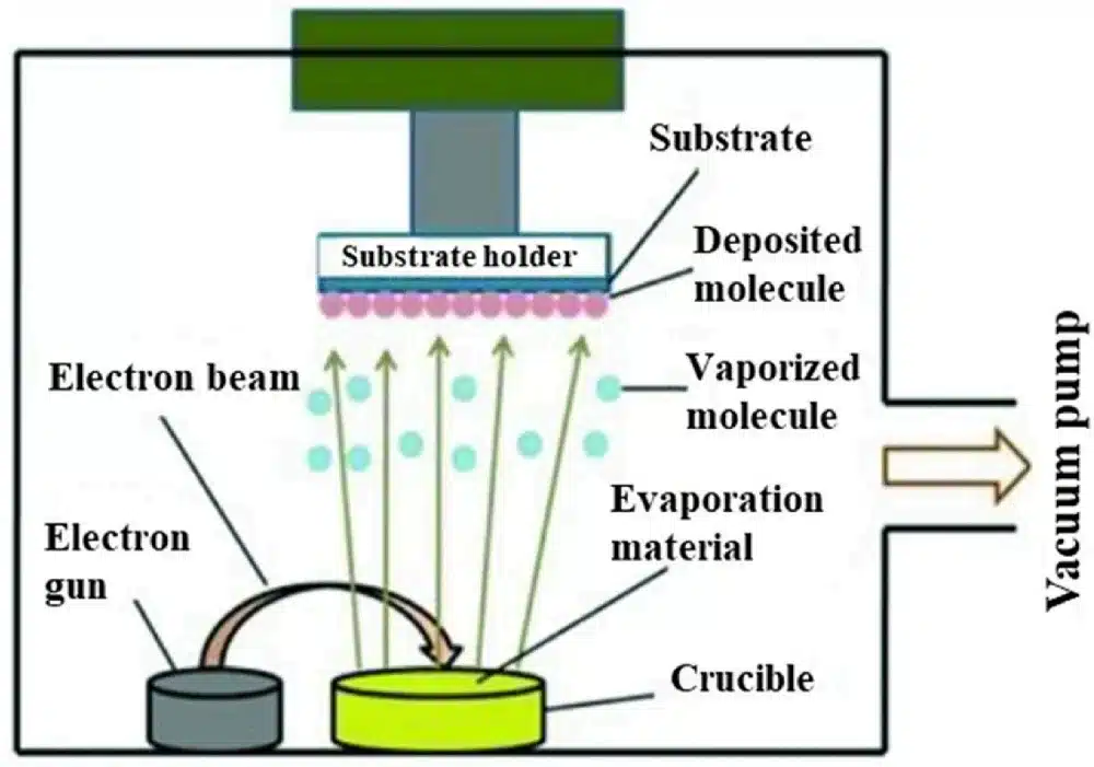
Key characteristics:
- Very high purity films (minimal contamination).
- Suitable for metals, metal oxides, semiconductors and organic molecules.
- Precise control of evaporation rate via beam power.
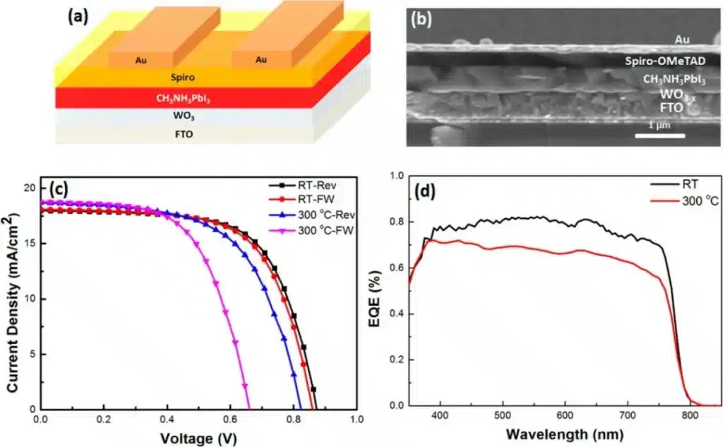
Example: WO₃₋ₓ thin films deposited on FTO glass by e-beam evaporation show improved electrical conductivity and photo-conversion efficiency as oxygen vacancy concentration increases, highlighting how deposition conditions tune functional properties.
3.3 Sputtering and Magnetron Sputtering
In sputtering, a plasma (typically argon) is ignited near a target (the source material). Positive ions from the plasma are accelerated toward the negatively biased target, physically knocking out atoms from its surface. These atoms then condense on the substrate.
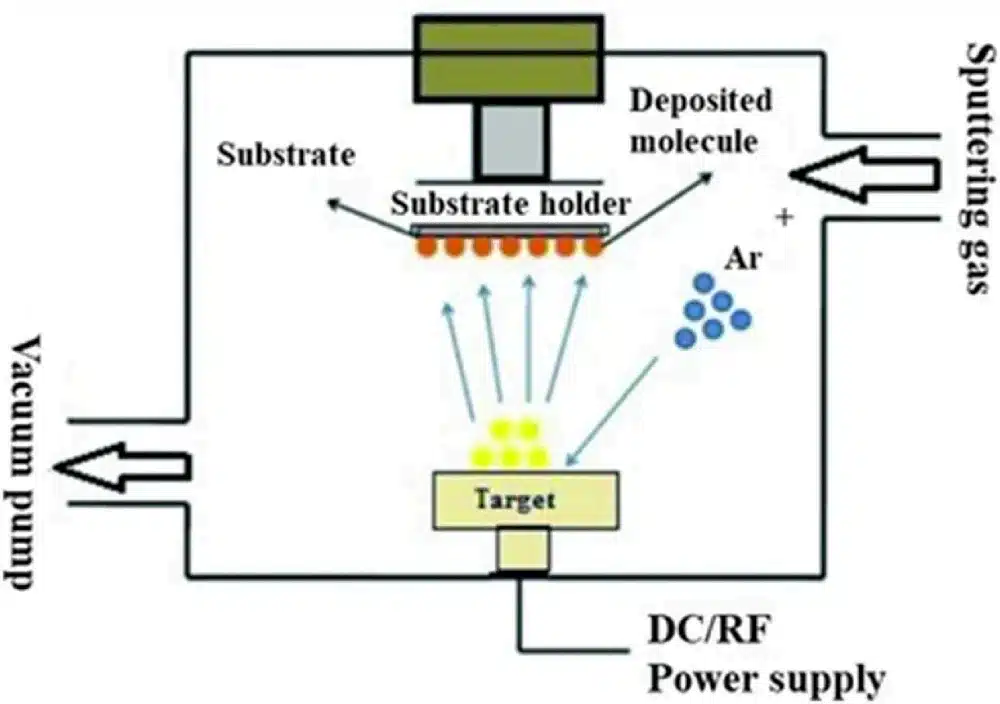
Important points:
- Ion bombardment also generates secondary electrons that help sustain the plasma.
- Sputtering works for conductive and insulating targets (with RF sputtering).
- Magnetron sputtering adds magnetic fields behind the target to trap electrons near the surface, increasing ionization efficiency and dramatically boosting deposition rate.
Example: RF magnetron sputtering of CZTS (Cu₂ZnSnS₄) films on soda-lime glass, followed by annealing at 350–550 °C, can produce kesterite-phase absorber layers for thin-film solar cells. Optimizing the Cu coverage ratio (e.g., 0.71) significantly improves optical properties.
薄膜.webp)
3.4 Advantages and Limitations of PVD
Advantages
- Atomic-level control over film composition, phase and thickness.
- High film purity and good adhesion.
- Wide material compatibility: metals, alloys, oxides, nitrides, multi-layer stacks.
Limitations
- Requires high vacuum and often elevated temperatures, increasing equipment and operating cost.
- Step coverage is relatively poor on very complex 3D structures.
- Coating rate, while high locally, can be limited over very large production areas.
4. Chemical Vapor Deposition (CVD)
4.1 Why CVD?
Chemical Vapor Deposition converts gaseous precursors into a solid film via chemical reactions at the heated substrate surface. It is widely used because it can produce dense, high-quality films at industrially relevant throughput and cost.
CVD performance is highly sensitive to:
- precursor chemistry and volatility
- gas-phase reactions and diffusion
- process parameters such as temperature, pressure, gas flow, viscosity and pH (for solution-based variants)
4.2 Generic CVD Process Steps
Despite many variations, most CVD processes follow the same basic sequence:
- Precursor delivery
- Reactive gases are introduced into the reactor and transported to the boundary layer above the substrate.
- Adsorption and surface reaction
- Precursors (and any gas-phase intermediates) diffuse through the boundary layer, adsorb on the heated substrate and undergo heterogeneous reactions (nucleation, growth, coalescence).
- Film growth and by-product removal
- A continuous film forms while gaseous by-products and any unreacted species desorb from the surface and are pumped away.
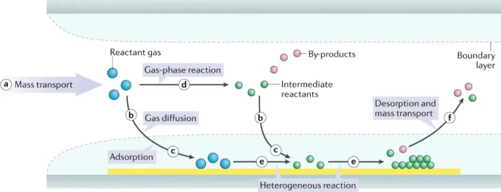
When temperature is sufficiently high or additional energy (e.g. plasma) is supplied, gas-phase reactions become significant. For catalytic substrates, surface-catalyzed reactions (like graphene growth on metals) dominate.
4.3 Plasma-Enhanced CVD (PECVD)
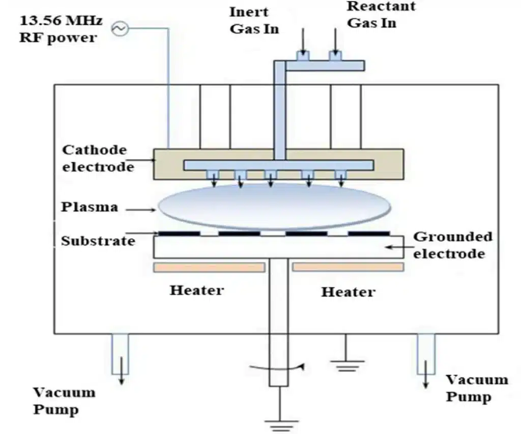
In PECVD, an RF power supply excites a plasma between electrodes. Reactive species generated in the plasma drive film formation at much lower substrate temperatures (typically 250–350 °C, instead of 600–800 °C in conventional thermal CVD).
Typical features:
- Suitable for temperature-sensitive substrates and previously processed devices.
- Widely used to deposit SiO₂, Si₃N₄, barrier layers, passivation layers and more.
- Process flexibility via RF power, pressure and gas composition.
4.4 Advantages and Limitations of CVD
Advantages
- High deposition rates and excellent film quality.
- Good conformality / step coverage, particularly in optimized low-pressure or PECVD processes.
- Scalable and repeatable for large-area production.
Limitations
- High process temperatures in many CVD variants, which may damage heat-sensitive substrates.
- Challenging to coat deeply shadowed or fully hidden surfaces.
- Reactor size and geometry can limit scalability for some architectures.
5. Atomic Layer Deposition (ALD)
5.1 Core Concept: Self-Limiting Surface Reactions
Atomic Layer Deposition can be seen as a special case of CVD where the surface chemistry is self-limiting. Precursors are introduced to the reactor sequentially, separated by inert gas purges, so they never overlap in the gas phase. This leads to:
- one or less than one monolayer added per cycle
- atomic-level thickness control
- outstanding conformality in ultra-high-aspect-ratio structures
5.2 Four-Step ALD Cycle
A typical ALD cycle consists of four steps:
- Precursor A exposure (chemisorption)
- The substrate is exposed to precursor A (Reactant 1). It reacts with surface functional groups until all reactive sites are consumed, releasing volatile by-products.
- Purge 1
- Inert gas removes excess precursor A and by-products from the reactor.
- Precursor B exposure (surface reaction)
- Co-reactant B is introduced and reacts with the chemisorbed layer of A in a self-saturating manner, completing one “atomic layer” of the target material and regenerating new surface groups.
- Purge 2
- Inert gas removes excess B and by-products, preparing the surface for the next cycle.
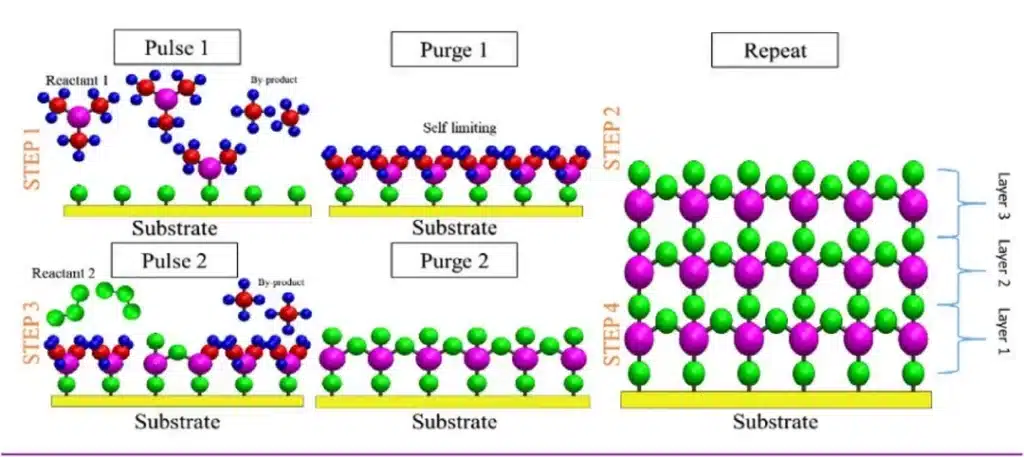
By repeating this cycle hundreds or thousands of times, ALD builds films with precise thickness and composition, even deep inside 3D nanostructures.
5.3 Thermal ALD vs Plasma-Enhanced ALD (PE-ALD)
ALD processes are typically categorized into:
- Thermal ALD (T-ALD) – relies purely on thermally activated surface reactions (150–350 °C typical).
- Plasma-Enhanced ALD (PE-ALD) – uses plasma to generate highly reactive species, allowing:
- lower deposition temperatures
- access to materials difficult for T-ALD
- improved film density or properties in some cases.
- uniform thickness for both methods;
- clear self-limiting behavior around 200 °C;
- higher growth per cycle (GPC) for PE-ALD (0.56 Å vs 0.38 Å at 200 °C), attributed to enhanced Nb adsorption in the plasma process.

5.4 Advantages and Limitations of ALD
Advantages
- Exceptional uniformity and conformality, even in deep trenches and porous structures.
- Atomic-scale control of thickness and stoichiometry.
- Can operate at relatively low temperatures, especially with PE-ALD.
- Self-limiting reactions yield excellent reproducibility and film quality.
Limitations
- Very low deposition rates (Å per cycle), so thick films are time-consuming.
- Precursors are often complex and expensive; ligands may be wasted.
- Process recipes are more complex and sensitive.
6. Choosing Between PVD, CVD and ALD
When deciding PVD vs CVD vs ALD for a specific project, consider the following factors:
6.1 Geometry and Step Coverage
- Simple or moderately complex geometry → PVD or CVD.
- High-aspect-ratio trenches, deep vias, porous structures → ALD (or CVD if conformality is sufficient).
6.2 Film Requirements
- Very dense, epitaxial or single-crystal layers → CVD (e.g., Si, SiC, GaN).
- Hard, wear-resistant or decorative coatings → PVD (e.g., TiN, CrN, DLC coatings).
- Ultra-thin barriers, gate dielectrics, ultra-conformal passivation → ALD / PE-ALD.
6.3 Temperature Budget
- Substrates that tolerate 600–800 °C → thermal CVD possible.
- Devices that must stay below 250–350 °C → PECVD, PE-ALD or some PVD processes.
6.4 Throughput and Cost
- Highest throughput / lowest cost per unit thickness → CVD, many PVD systems.
- Highest precision, but lowest throughput → ALD.
7. From Thin Films to Real Components: Why This Matters
For engineers working with metal components, molds and die cast parts, thin-film deposition is not just academic:
- PVD coatings like TiN, CrN, TiAlN, or DLC are widely used to improve wear resistance, corrosion resistance and friction behavior on tooling and precision parts.
- CVD and PECVD layers provide electrical insulation, barrier layers and passivation in power devices, sensors and complex assemblies.
- ALD barrier films are increasingly used in advanced packaging and high-density electronics where leakage and reliability are critical.
Understanding the fundamentals of PVD, CVD and ALD helps you:
- talk to coating vendors using the right technical language;
- choose realistic coating specs (thickness, roughness, temperature limits);
- evaluate trade-offs between cost, performance and lead time.
8. Conclusion
PVD, CVD and ALD are not competing buzzwords – they are complementary tools in the thin-film toolbox:
- PVD excels at high-purity, high-rate coatings on relatively simple surfaces.
- CVD / PECVD balances throughput and quality, delivering dense films with good conformality.
- ALD / PE-ALD is the method of choice when you need atomic-level control and perfect coverage in complex 3D structures.
By understanding the strengths and limitations of PVD vs CVD vs ALD, you can better match each deposition method to the geometry, material, and performance requirements of your next device or component.
Surface Treatment Services with Certified Quality and Environmental Management
Beyond thin film deposition technologies such as PVD, CVD and ALD, our team also provides comprehensive surface treatment services for metal and precision-engineered components. From cleaning, polishing and blasting to protective and decorative finishes, every process is controlled to enhance durability, corrosion resistance and functional performance.
Our facilities are certified to ISO 9001:2015 for quality management and ISO 14001 for environmental management. This ensures stable process control, full traceability and environmentally responsible operations across all surface treatment projects, so your parts achieve consistent appearance and performance while meeting global regulatory requirements.
Aluminum Die Casting Services
Learn more about our aluminum high pressure die casting services in China.

